
METALLURGICAL TESTING
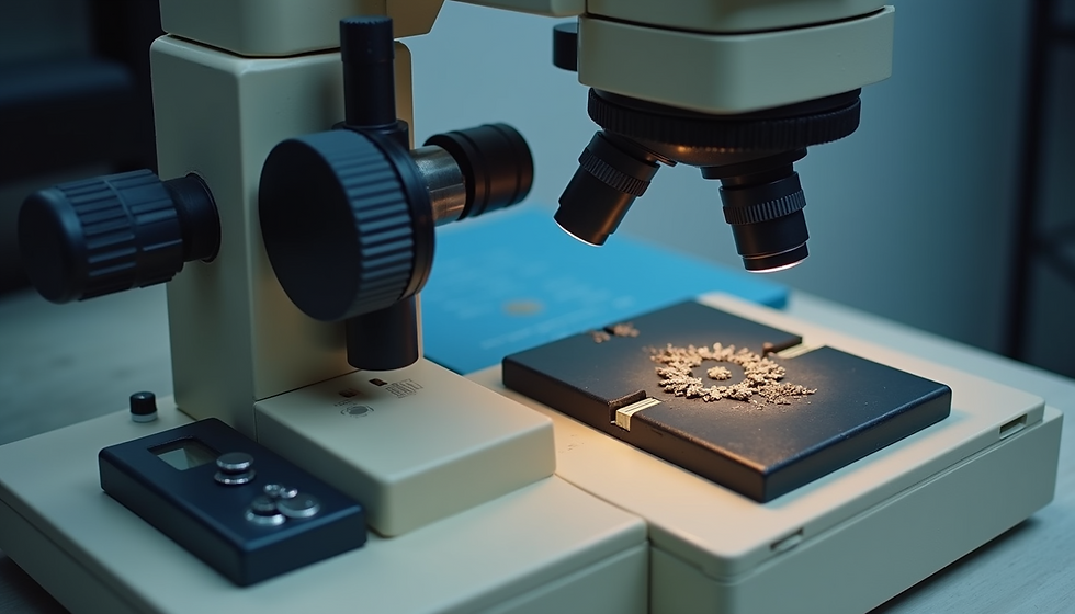
UPRIGHT METALLURGICAL MICROSCOPE AND STEREOSCOPE

-
Fully automated upright metallurgical microscope
-
Make – : Zeiss.
-
Model -: M TO M.
-
Magnification from 25X to 1000X.
-
Auto stich facility to more field of view at high magnification.
-
Auto Technical Cleanliness in single scan (Millipore test) as per ISO 16232, ISO 4406, VDA 19.1.
-
Graphite analysis as per ASTM A247 , ISO 945.
-
Auto measurement of Nodule count , Nodularity , Size , Class , Graphite form and distribution.
-
Auto grain size measurement as per ASTM E112 , ISO 643.
-
Auto grain measurement as per comparison , intercept and planimetric
-
Grain size templates available in the Zeiss software for auto comparison.
-
Multi-phase analysis.
-
Volume fraction of phases as per ASTM E562 manual and Auto.
-
Coating thickness measurement.
-
Auto Non -metallic inclusion analysis as per ASTM E45, IS 4163, ISO 4967 and DIN 50602(K1,K2,K3 and K4).
-
Auto porosity analysis as per ASTM E2109.
-
Autofocus and Extended depth of focus.
-
Stereoscope with magnification from 7.5X to 45X to cater the images of fracture specimen and weld.


SCANNING ELECTRON MICROSCOPE
Facility Details Model: EVO 10 Make: ZEISS, Germany
Instrument Specifications
• Magnification Range: Up to 500,000×
• Resolution: o3 nm @ 30 kVo8 nm @ 3 kV
• EDS-System: Xplore 30 EDS detector (Oxford Instruments)
• Detectors Available:
• Secondary Electron (SE) Detector
• Backscattered Electron (BSE) Detector EDS
Key Features of NPTCS
• Working Hours: 9:30 AM to 6:00 PM
• Fast and accurate analysis
• Expertise in failure analysis and result interpretation
• Reliable support from experienced technical professionals
Capabilities
• High-resolution surface morphology imaging
• Elemental and chemical composition analysis at pinpoint locations
• Suitable for both conductive and nonconductive materials
Typical Uses
• Fractography and failure analysis
• Particle analysis
• Milipore Test Paper Scan for Particle size and particle identification
• Micro-level chemical composition analysis
• Defect and surface evaluation Applications / Suitable Industries
• Metal and non-metal industries
• Ceramic industries
• Polymer, plastic, and rubber industries
• Biomedical applications (dental materials and implants)
• Electronic and semiconductor industries
• General material characterization and research